
The scientific program of ORIGENAL is organized in three work packages (WP):
The goal of WP1 is to develop the thin-film-transistor (TFT) technology needed for fabricating integrated circuits on foil-based substrates.
The materials of choice are laminated, few-layered transition-metal-dichalcogenides (TMDCs) semiconductors, such as MoS2 and WSe2.There are a several reasons that make these two-dimensional (2D) semiconductors ideal candidates for ultra-scaled digital devices on flexible substrates:
- Their two-dimensional nature allows higher foldability than the traditional high-end semiconductors.
- They are compatible with the standard low-temperature deposition and patterning techniques required for foil-based technology and have significantly higher charge-carrier mobility than other low-temperature-compatible materials, such as polymers.
- They provide significantly high tolerances for the short channel effects.
TMDC transistors have been demonstrated on rigid substrates and on foil, showing the great potential of these devices for logic applications. TU Wien has already developed a MoS2 NMOS-technology that allowed realizing a microprocessor with 115 transistors. In the ORIGENAL project, we will extend this fabrication process and complement it with know-how from flexible graphene devices, to make it compatible with flexible foil substrates such as ultrathin PEN or PET. This approach will provide a fast route for the development of a digital library regarding the 2D components and the compatible folding processes.
At the same time, we will develop p-type transistors based on TMDC semiconductors such as WSe2, to enable the fabrication of CMOS circuits. In general, CMOS is preferred over NMOS because of lower static power consumption, higher gain/noise margin in logic stages and smaller footprint. One of the objectives of WP1 is the design and development of integrated CMOS circuits for memory applications.
WP Coordinator: Thomas Mueller (TU Wien)
WP2 will use a multi-scale approach (ranging from ab-initio calculations to circuit simulation netlists) to assess the potential of electronic devices based on 2D materials, with the scope of:
- providing guidelines to the fabrication side,
- realizing a digital library for high-performance analog and digital circuits based on 2D devices and 3D stacked architectures.
Simulations have already been used to investigate the performance of field effects transistors (FETs) based on TMDCs in the best case scenario, i.e. considering ideal and perfect devices. Here we’ll extend these preliminary studies to take into account the presence of non-idealities such as defects, ionized impurities and strain, to evaluate the performance of the devices in realistic conditions. The results will be transferred into circuit-level design guidelines. We will employ a closed feedback-loop between simulations and device fabrication and testing, using the results of the simulations as guidelines for fabrication, and comparing theoretical and experimental results to continuously improve our models.
Furthermore, will create a digital library comprising both basic logic elements based on 2D devices, and deep and intervening interconnects implemented in the 3D architecture. We will investigate the balance between internal gate-level routing and block or chip-level interconnections in the 3D architecture to optimize the transistor density and network speed. A new type design partition between logic gates and hierarchical blocks (like ALUs, registers, memories) level will be introduced to take full advantage of the 3D integration concept.
WP Coordinator: Gianluca Fiori (Uni Pisa)
WP3 represents the core activity of the ORIGENAL project. It includes:
-
- The development of a dedicated film stack formed by a thick handling foil, a conductive layer for electrodeposition of metals, the substrate foil for the electronic circuits and a release adhesive between the layers.
- The development of a fabrication technology for through-foil vias, to provide electric contact between two layers folded on each other.
- The fabrication of a proof-of-concept demonstrator based on the existing roll-based nanolithography setup at VTT, to test and demonstrate the folding processes and to provide information on the practical challenges.
- The conceptual design of a tool capable of folding with the desired accuracy (μm scale) and the ability to make intervening connections inside the folded stack, using only processes compatible with the electronics on the foil with regards of the thermal budget and chemistry.
In principle, there are (at least) three different possible arrangements for folding, as schematically illustrated below. The “rolling-up” is the approach currently used for foil capacitors. It enables a very high through-put, but it is associated with significant challenges related to alignment and changing bend radius.
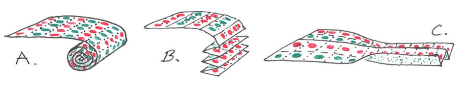
In ORIGENAL the focus will be on the type of origami-folding illustrated in Figure (b) and (c), which maintains the structure of the final element regardless of the length of the roll (full scalability in length). It is also expected to allow more accurate alignment than the traditional sheet-to-sheet stacking, as the structures to be aligned are fabricated in close proximity to each-others. The miniature size of the folds may even allow the use of self-aligning and self-folding techniques for optimal scalability.
WP coordinator: Sanna Arpiainen (VTT)